General Notion
In this article I’d like to give some introduction to Garbled Circuits. If you have reached to this article and are wondering what is a Garbled Circuit, you are probably at least somewhat familiar with Multiparty-Computation and cryptography.
To make things clear, let’s say that MPC is a sub-domain of cryptography that deals with methods which allow a set of mistrusting parties, each holding its own input, to compute a function of those inputs such that none of the parties learn anything about the (private) input of the other parties, besides what can be trivially inferred about it from the output.
For example, consider Yao’s Millionaires Problem in which a two millionaires would like to know which of them is richer without disclosing their fortune.
Each millionaire’s input would be the value of its fortune and the function to be evaluated (which returns either True or False) is whether the first input is bigger than the second input.
Now that the setting is clearer, I can say that Garbled Circuits is a protocol, allowing two parties $\mathcal{P}_A,\mathcal{P}_B$ with inputs $i_A,i_B$ respectively, to compute a function of their inputs: $f(x,y)$ such that each party will learn only $f(i_A,i_B)$. How awesome is that?
Goal and Non-Goals
In this article I’d like to give some sense about how Garbled Circuits are built and how does the magic work. I’ve found this topic tends to be cryptic to some friends and colleagues and thought creating this document will give some intuition about the building blocks of GCs. This article does not intend to be rigorous and I’ll not be proving any security property of GCs. I find learning crypto topics as a multi-tiered-procedure, where first gaining a general sense about the cryptographic entity and only later giving a more explicit, rigorous and formal definitions and proofs about this entity makes complex topics easier to grasp. I will also not consider some extensions of GCs for more than two parties while such extensions do exist. The interested reader can refer to Oded Goldreich’s article to learn more about it. Notice that Oded is using the term “Scrambled Circuit” instead of a “Garbled Circuit”.
Security Assumptions
In this article we assume the Semi-Honest model of security. By making this assumption we disregard any scenario in which one of the parties deviates from an agreed-upon protocol to gain extra information. In other words, we assume the parties are honest-but-curious, so they follow the protocol precisely as stated but may be interested in gaining extra information from the messages they receive along the process. We will explain why such honest-but-curious parties may not gain any information except for the output of the function being computed (without too much formality involved). We will not approach the more complex problem of building a GC protocol in the Malicious-Adversary model, where paries may deviate from the prescribed protocol arbitrarily.
Building Garbled Circuits
Setting
The collaborting parties $\mathcal{P}_A, \mathcal{P}_B$ hold inputs $A,B$ respectfully and wish to jointly compute a function $f(A,B)$. The inputs $A,B$ are represented each as a vector of bits. When building a Garbled Circuit for the function $f$ the first thing one does is representing $f$ as a boolean circuit, composed of boolean gates. For simplicity we will deal with two types of gates:
- And Gates, which compute the logical AND of its two input bits:

- XOR Gates, which compute the logical exclusive-OR of its two input bits:

It is a well-known result that any boolean function can be represented as a boolean circuit composed only of AND gates and XOR gates. Therefore, if we can show that the XOR and AND gates can be computed by two parties such that the input privacy is preserved, and that we securely compose these gates we can achieve our desired goal.
We will not discuss how can a function be represented as a boolean circuit, as this for itself is an active research field. Thus at this point we will simply assume that such representation does exist for our given function.
To make the construction more concrete and approachable and we will discuss a specific instance of the problem for a rather simple function $f$. Later, we give a generalized algorithm for any function. The function we will deal with in our construction is the function that takes two numbers of two binary digits each and tells whether they are the binary negation of each other. In other words, if the first input is equal to the number obtained by taking the second input and flipping all the bits representing it. For example, $f(2,1)=1$ because 2’s binary representation is 10 and 1’s binary representation is 01, and since 10 is obtained by flipping all the bits in 01 then $f(2,1)=1$. To be precise, the numbers (inputs) of the parties will be $A=(a_0,a_1)$ and $B=(b_0,b_1)$ where $a_0,a_1,b_0,b_1$ are bits and $A,B$ are the input numbers with the binary representation of $a_1a_0$ and $b_1b_0$ respectively. The single bit of output of the function is $C=(c_0)$. For example, if the input of party $\mathcal{P}_A$ is the number $2$, is will be represented as $A=(0,1)$ and the input of party $\mathcal{P}_B$ is the number $1$. Then the output of the function will be $C=(1)$.
The boolean circuit for the additional function is:
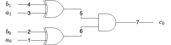
We have annotated each wire with a number which we will use later in our building.
General Approach
In this subsection we’ll try to build a GC for our function $f(A,B)$ taking as input two vectors of two bits each, representing two numbers, and sending as output a “vector” of a single bit. In the beginning we have two parties who have the boolean circuit for $f$. Now, let’s think, if we were trying to solve this problem ourselves what would be the first thing we were trying to tackle? Well, since none of the parties can learn nothing besides the output of the computed function, party $\mathcal{P}_A$ can’t simply send its input $A$ to party $\mathcal{P}_B$. If it did, party $\mathcal{P}_B$ could compute $f(A,B)$ and send it to $\mathcal{P}_A$, but by doing so $\mathcal{P}_B$ would also learn $A$, the input of $\mathcal{P}_A$ which violates our privacy requirements. Therefore, the information $\mathcal{P}_A$ should send to $\mathcal{P}_B$ shall not disclose its input but would still allow $\mathcal{P}_B$ to evaluate the function. So, the approach we shall take is a little bit different. Instead, $\mathcal{P}_A$ will send a garbled version of the circuit to $\mathcal{P}_B$ and some “instructions” for $\mathcal{P}_B$ about how to “translate” its input ($B$) into the garbled circuit. Next, $\mathcal{P}_B$ will evaluate the garbled circuit which would yield a garbled output, and send this output to $\mathcal{P}_A$, who will ungarble the garbled output into the correct output and send it to $\mathcal{P}_B$. Garbling the circuit, done by $\mathcal{P}_A$ will require:
- Garbling each gate.
- Garbling the input.
In the following subsections we will explain how these can be done.
Garbling a Single Gate
Let’s consider a logical gate with two input wires $(w_a,w_b)$ and a single output wire $(w_c)$. So when the values that are fed into the input wires are set to specific values, the output wire will hold the correct value obtained from applying the logical function of the gate on the values fed into it from the two input wires. The functionality of the logical gate can be described using a truth table, a table which gives the value of the output wire $(w_c)$ to each of the possible four combinations of the input wires $w_a, w_b$. For example, the truth table of a logical-AND gate we have in our boolean circuit is the following:
| $w_a$ | $w_b$ | $w_c$ |
|---|---|---|
| 0 | 0 | 0 |
| 0 | 1 | 0 |
| 1 | 0 | 0 |
| 1 | 1 | 1 |
To make things clear, the first line in the table, for example, means that if the input wires w_a and w_b take the values of and , than the output wire $w_c$ will take the value of as well, which is the logical-AND of the two inputs. While it’s a common practice, it’s important to recall that the value of represents a logical “False” and the value of 1 is representing a logical “True”.
The truth table of a logical-XOR gate is the following:
| $w_a$ | $w_b$ | $w_c$ |
|---|---|---|
| 0 | 0 | 0 |
| 0 | 1 | 1 |
| 1 | 0 | 1 |
| 1 | 1 | 0 |
First Attempt
How Does it Work
We will garble the truth table by assigning two encryption keys to each wire in the circuit. So, for example consider our circuit with seven different wires, thus we will generate for each wire $i$ two keys $K_i^0$ and $K_i^1$. Intuitively, we need two keys to represent the two possible states of the wire, where it either carries the value of “0” or the value of “1”. The keys are of a symmetric encryption scheme, so the key is used both for encryption and decryption. Let’s zoom-in on a specific gate in the circuit, for instance, our logical XOR gate with input wires 1 and 2 and output wire 6. Wire 1 will have two keys $K_1^0$ and $K_1^1$. Wire 2 will have two keys $K_2^0$ and $K_2^1$ and output wire 6 will have two keys for it $K_6^0$ and $K_6^1$. Next, we can garble the truth table in the following way. For each line in the original (ungarbled) truth table, taking input values $x$ on wire 1 and $y$ on wire 2 and mapping them into output $z$ on wire 6 ($x,y,z$ are all one bit wide) we can create a line in the garbled truth table mapping $K_1^{x}$ and $K_2^{y}$ to $K_6^{z}$. For example, the second line in our logical-XOR gate truth table, we had inputs $x=0$ and $y=1$ mapped to the output $z=1$ (because 0 XOR 1 = 1), in the garbled table we will have $K_1^0$, $K_2^1$ map to $K_6^1$. The full garbled table of the logical-XOR will be:
| Wire 1 | Wire 2 | Wire 6 |
|---|---|---|
| $K_1^0$ | $K_2^0$ | $K_6^0$ |
| $K_1^0$ | $K_2^1$ | $K_6^1$ |
| $K_1^1$ | $K_2^0$ | $K_6^1$ |
| $K_1^1$ | $K_2^1$ | $K_6^0$ |
The garbling of the input is done so that for each input wire of $\mathcal{P}_A$, the party $\mathcal{P}_A$ will send the key representing the garbling of the input. For example, our XOR gate with input wires 1 and 2 and output wire 6 we know the value of wire 1 is part of the input of party $\mathcal{P}_A$. Now if the input of party $\mathcal{P}_A$ for this bit is $0$, then the garbled value of it will be $K_1^0$ and if the input is $1$ then it will be garbled to $K_1^1$ where keys $K_1^0,K_1^1$ and the two keys associated with wire $1$. Notice that party $\mathcal{P}_B$, who receives the garbled input can’t tell whether it represents the garbling of or $1$, because both keys are just random numbers and $\mathcal{P}_A$ didn’t share with $\mathcal{P}_B$ the meaning of key.
Now in order to compute the output of the gate, party $\mathcal{P}_A$ will send to $\mathcal{P}_B$:
- The garbled truth table for each gate.
- The garbling of its input bits for each wire on which the inputs of party $\mathcal{P}_A$ appear.
- The two keys associated with each input wire of party $\mathcal{P}_B$ so it will be able to translate its input to the input the garbled circuit is expecting.
Also notice that $\mathcal{P}_A$ must sent both keys for each wire since $\mathcal{P}_B$ can’t just tell $\mathcal{P}_A$ what its input bit is, as this will violate our privacy requirements.
The Issues With it
As good as it may sound, things don’t end here, since at this point in order to evaluate the gate, $\mathcal{P}_B$ receives the garbling of $\mathcal{P}_A$’s input and the problem is that while $\mathcal{P}_B$ will be able to evaluate the gate, it will also be able to derive whether $\mathcal{P}_A$’s input to our XOR gate is $K_1^1$ or $K_1^0,$ thus inferring the value of the ungarbled input of $\mathcal{P}_A$.
This is possible since the ordering of the rows is such that in the first and second rows the ‘Wire 1’ column contains $K_1^0$ and in the third and forth rows it contains $K_1^1$ so $\mathcal{P}_B$ can just compare the key it got with the values in these rows and ascertain the input of $\mathcal{P}_A$ which violates our privacy requirements!
So, one thing we have to do is mix the ordering of the lines randomly. After mixing the rows, the garbled table of our XOR gate looks like this to $\mathcal{P}_B$.
| Wire 1 | Wire 2 | Wire 6 |
|---|---|---|
| $K_1^?$ | $K_2^?$ | $K_6^?$ |
| $K_1^?$ | $K_2^¿$ | $K_6^¿$ |
| $K_1^¿$ | $K_2^?$ | $K_6^¿$ |
| $K_1^¿$ | $K_2^¿$ | $K_6^?$ |
For completeness, the garbled table of the AND gate (with input wires 5,6 and output 7) is:
| Wire 5 | Wire 6 | Wire 7 |
|---|---|---|
| $K_5^?$ | $K_6^?$ | $K_7^?$ |
| $K_5^?$ | $K_6^¿$ | $K_7^?$ |
| $K_5^¿$ | $K_6^?$ | $K_7^?$ |
| $K_5^¿$ | $K_6^¿$ | $K_7^¿$ |
We use the notation of “?” and “¿” to denote that $\mathcal{P}_B$ simply doesn’t know what is the meaning of the value.
However, even if we mix the rows, $\mathcal{P}_B$ can still reveal the whole input of party $\mathcal{P}_A$. One possible attack that can be done on the AND gate is by exploiting its asymmetry in its output column of wire 7. Since this output column (of wire 7) has three rows with the same value and one row with another value, by knowing the functionality of AND gate we can tell that this last value represents a logical 1 (since only one combination of the inputs to a logical AND gate can yield the output of 1). After $\mathcal{P}_B$ derives the values of $K_7^1$ and $K_7^0$ it can also tell that the two keys of the wires 5 and 6 that yield the output of $K_7^1$ must be $K_5^1$ and $K_6^1,$ and thus $\mathcal{P}_B$ can also derive the values of $K_5^0,K_5^1,K_6^0,K_6^1$. At this point, going back to the XOR gate (with input wires $1,2$) $\mathcal{P}_B$ can tell, even without enumerating all the inputs, that if the XOR of the value it provided $(b_0)$ with the one $\mathcal{P}_A$ provided $(a_0)$ yields the $K_6^1$ then $b_0$ and $a_0$ are different and if it yields the value of $K_6^0$ with $a_0$ and thus it can infer the value of $a_0$ and learn the input of $\mathcal{P}_A$.
The issue stems from the fact that $\mathcal{P}_B$ has been able to exploit some asymmetry at the output of the AND gate. Thus, we must have each output of the garbled circuit appear only once so $\mathcal{P}_B$ should not be able to exploit such asymmetries.
Second attempt
How Does it Work
This time, just like the previous one $\mathcal{P}_A$ will assign two encryption keys for each wire in the circuit, so we will use the name notation like in the previous attempt.
However, this time instead of submitting a table for each gate with multiple columns, it will send only the output column of the truth table and each output will be encrypted with the two keys of its corresponding inputs. For example, the table for the XOR gate (with input wires $1,2$) will look like this (but don’t forget $\mathcal{P}_A$ also shuffles the rows before sending them):
| Wire 6 |
|---|
| $E_{K_1^0}(E_{K_2^0}(K_6^0 || K_6^0)$ |
| $E_{K_1^0}(E_{K_2^1}(K_6^0 || K_6^0)$ |
| $E_{K_1^1}(E_{K_2^0}(K_6^0 || K_6^0)$ |
| $E_{K_1^1}(E_{K_2^1}(K_6^1 || K_6^1)$ |
We denote with $x|y$ the concatenation of strings $x,y$. We also denote with $E_K(p)$ the encryption of $p$ with key $K$.
So each output is the double encryption (using the key of the first input wire and then the second input wire) of the concatenation of the output with itself. We’ll explain shortly why we concatenate the output with itself, but for now take it as given.
And $\mathcal{P}_2$ views this table as:
| Wire 6 |
|---|
| $E_{K_1^?}(E_{K_2^?}(K_6^? || K_6^?)$ |
| $E_{K_1^?}(E_{K_2^1}(K_6^? || K_6^?)$ |
| $E_{K_1^¿}(E_{K_2^?}(K_6^? || K_6^?)$ |
| $E_{K_1^¿}(E_{K_2^¿}(K_6^¿ || K_6^¿)$ |
So this time, just like previous attempt $\mathcal{P}_A$ will send:
- The garbled output column for each gate.
- Its garbled input of each input wire $\mathcal{P}_A$ feeds.
- The two input-encryption keys of $\mathcal{P}_B$, (in our case: $K_2^0,K_2^1,K_4^0,K_4^1$) just like previous attempt. $\mathcal{P}_A$ will also send to $\mathcal{P}_B$ its garbled input for wires $1,3$ which are $K_1^{a_0}$ and $K_3^{a_1}$.
Now, for our XOR gate (with input wires 1 and 2) $\mathcal{P}_B$ will take $K_1^?$ (just like we did before, we use “?” to imply that $\mathcal{P}_B$ doesn’t know whether its the garbling of the value “1” or “0”) and its own garbled input (let’s assume its $K_2^0$ without loss of generality). Next, it will try to double-decrypt all the entries in the garbled table with the input encryption keys until the decryption successfully results in some value written twice (with $K_6^? || K_6^?$ or $K_6^¿ || K_6^¿$), in this case it knows that the resulting output is correct. So, we write the output value twice as a way to verify that a decryption is successful so $\mathcal{P}_B$ can tell that the output is correct. There are other ways of doing the kind of verification that the decryption is done correctly, see Authenticated Encryption for further detail.
For example, if $\mathcal{P}_A$’s garbled input is $K_1^1$ and $\mathcal{P}_B$’s garbled input is $K_2^0$ then $\mathcal{P}_B$ will try to decrypt each entry in the garbled table as follows:
- It Will compute $D_{K_2^0}(D_{K_1^1}(E_{K_1^?}(E_{K_2^¿}(K_6^? || K_6^?))))$, where $D_K(c)$ denotes the decryption of ciphertext $c$ with key $K$.
- If the result is the repetition of some string with itself $K_6^? || K_6^?$, $\mathcal{P}_B$ can tell that this string is the garbled output of the gate and will keep $K_6^?$.
- If not, will try the next value in the table. For one of the entries in the table the check must succeed.
The Issues With it
The only issue we have arises from the fact that $\mathcal{P}_B$ receives the garblings of both of its possible inputs for each wire that its input feeds, so it can enumerate all possible combinations of its inputs and evaluate the circuit for each such combination. We know that for all input combinations, except for one, the output will be the same (the value of $K_7^0$) and only for one of the combinations the output will be unique ($K_7^1$), this is because only for one possible input of $\mathcal{P}_B$, which is the negation of the input of $\mathcal{P}_A$, the circuit will output the value of 1. By taking the input that was fed into the circuit to yield the unique value of $K_7^1$, ungarbling it and flipping the bits $\mathcal{P}_B$ can reveal the whole input of $\mathcal{P}_A$, which violates our privacy requirements.
Conclusion
We understand that $\mathcal{P}_B$ can’t receive both keys for each wire that it feeds its input, because then it will be able to learn \mathcal{P}_A’s input. However, without those keys - it must disclose its input to $\mathcal{P}_A$! How can we solve it? While it may seem like a dead end - luckily cryptographers have come up with a great solution, known as “Oblivious Transfer”.
Oblivious Transfer (OT)
Definition
The problem oblivious transfer (OT) is trying to solve is the following:
There are two parties $\mathcal{P}_A$ and $\mathcal{P}_B$. Party $\mathcal{P}_A$ is holding two values $x_1,x_2$. Party $\mathcal{P}_B$ is holding a bit $b$. The parties want $\mathcal{P}_B$ to learn $x_b$ without $\mathcal{P}_A$ learning the value of $b$ (i.e. which $x_b$ was transferred to $\mathcal{P}_A$).
While it isn’t very complex, we will show go through the construction of Oblivious-Transfer in this post(please let me know if you find this topic interesting, I may create another post about it later). This post is complex enough :)
Last and Working Attempt
This attempt will be exactly like the second attempt, but we will leverage OT to solve our last problem. The only difference from previous attempt will be that now $\mathcal{P}_B$ will learn only one of either $K_2^0$ or $K_2^1$ and either $K_4^0$ or $K_4^1$, according to what $\mathcal{P}_B$’s input is. This will be done using Oblivious-Transfer. This prevents the attack suggested in the previous attempt since now $\mathcal{P}_B$ will hold only one of $K_2^0$ and $K_2^1$ and only one of $K_4^0$ and $K_4^1$.
The Full Algorithm
Just to recap over our amazing result, this subsection will give the full details of our garbled circuits.
Setting
There are two parties $\mathcal{P}_A$ and $\mathcal{P}_B$ with bit-vector inputs ${\bf A} = (A_1,…,A_n)$ and ${\bf B}=(B_1,…,B_n)$ respectively. A function $f$ represented as a boolean-circuit, known to both parties with wires $w_1,w_2,…,w_k$ where $k$ is the total number of wires in the circuit. Wires $w_1,…,w_n$ will be the $n$ wires in the circuit that take the input of $\mathcal{P}_A$.
The next $n$ wires, $w_{n+1},…,w_{2n}$, will take the input of $\mathcal{P}_B$. The rest of the wires take the output of one of the gates in the circuit. The goal of both parties is to evaluate $f$ together without disclosing any information about their inputs.
The evaluation works in three phases:
- Garbling Phase, in which $\mathcal{P}_A$ will garble both its input and the circuit of $f$ will send all the garbled content to $\mathcal{P}_B$. In this phase $\mathcal{P}_B$ will also obtain the garbling of its input from $\mathcal{P}_A$ using OT.
- Evluation Phase, in which $\mathcal{P}_B$ will evaluate the garbled circuit to obtain a garbled output, which will be sent to $\mathcal{P}_A$.
- Output Phase: $\mathcal{P}_A$ will ungarble the output of the circuit and send the ungarbled output to $\mathcal{P}_B$.
Garbling Phase
Party $\mathcal{P}_A$ will garble the circuit and its input. Each wire $w_j$ in the circuit will be assigned with two encryption keys $K_j^0$ and $K_j^1$ which will represent the garbling of the values of and 1 going through the wire, respectively. Next, for each gate $G$ in the circuit with two input wires $w_a, w_b$ and one output wire $w_c$ with the following truth table:
| $w_a$ | $w_b$ | $w_c$ |
|---|---|---|
| 0 | 0 | $g_{0,0}$ |
| 0 | 1 | $g_{0,1}$ |
| 1 | 0 | $g_{1,0}$ |
| 1 | 1 | $g_{1,1}$ |
Such that $g_{i,j}$ is the output of the gate $G$ with inputs $w_a=i$ and $w_b=j$. Then the garbling of gate $G$ with the truth table above is:
| $w_c$ |
|---|
| $E_{K_a^0}(E_{K_b^0}(K_c^{g_{0,0}} || K_c^{g_{0,0}}))$ |
| $E_{K_a^0}(E_{K_b^1}(K_c^{g_{0,1}} || K_c^{g_{0,1}}))$ |
| $E_{K_a^1}(E_{K_b^0}(K_c^{g_{1,0}} || K_c^{g_{1,0}}))$ |
| $E_{K_a^1}(E_{K_b^1}(K_c^{g_{1,1}} || K_c^{g_{1,1}}))$ |
Each garbled gate will be sent to $\mathcal{P}_B$. The input of $\mathcal{P}_A$, which is ${\bf A} = (A_1,…,A_n)$ will be garbled into $(K_1^{A_1},…,K_n^{A_n})$. The garbled input vector will also be sent to $\mathcal{P}_B$.
After receiving the garbled circuit and the garbled input of $\mathcal{P}_A$, the parties will run $n$ iterations of the OT protocol so $\mathcal{P}_B$ will learn its garbled input $K_{n+1}^{B_1},…,K_{2n}^{B_n}$.
Evaluation Phase
At this point $\mathcal{P}_B$ will evaluate the circuit by sequentially evaluating each gate in the circuit, starting from gate that depends only on the inputs of the parties up until evaluating the gate which yield the output of the function. For each gate with input wires $w_a, w_b$ and output wire $w_c$ we assume that the garbled value of both input wires are already known, either because these are the input wires or because they are wires who come out of a gate which was already evaluated. The value of each wire $w_a$ is one of the encryption keys associated with the wire, either $K_a^0$ or $K_a^1$.
Since the circuit is garbled $\mathcal{P}_B$ doesn’t know which value of those is he holding so we denote the values he holds in his perspective as $K_a^?$ and $K_b^?$. Then, party $\mathcal{P}_B$ will decrypt, using the keys from the input wires, all entries in the table until the decryption yields some string which is repeated twice $K_c^? || K_c^?$. When it does, $\mathcal{P}_B$ can tell that the decryption succeeded and the garbled output of the gate is the $K_c^?$ retrieved from the decryption. When the decryption succeeds $\mathcal{P}_B$ sets the value of $w_c$ to be $K_c^?$ and moves on to evaluate ther next gate. When it finishes evaluating all gates in the circuit it will send the garbled value of the output wires to party $\mathcal{P}_A$.
Output Phase
Party $\mathcal{P}_A$ receives the garbled output of each wire. Using the keys it generated for each wire it can tell whether each value is the garbling of 1 or 0 and thus construct the (ungarbled) output and share it with $\mathcal{P}_B$.
Summary
In the article we’ve discussed what garbled circuits are, their usage and purpose and how they can be constructed. The academic community has put a lot of effort into understanding and optimizing garbled circuits and many optimizations exist which greatly reduce the communication complexity of the parties as well allow ensuring certain security properties. In particular some security and integrity properties of the process aren’t guaranteed with our existing construction:
- How can party $\mathcal{P}_B$ know that the garbled circuit represents the original circuit?
- How can party $\mathcal{P}_A$ know that the output it receives really is the output of the circuit?
Moreover, we haven’t discussed the construction of OT which solved one of the core issues in our construction. Maybe I’ll discuss those in a future post.
See you next time!